
Aluminum Framed SMT PCB Stencils for PCB Assembly
Product Description
The sole purpose of an SMT stencil is to transfer solder paste to a bare circuit board. A stainless steel foil is laser cut creating an opening for every surface mount device on the board. Once the stencil is properly aligned on top of the board, solder paste is applied over the openings (making a single pass, using a metal squeegee blade). When the stainless steel foil is separated from the board, solder paste will remain, ready for placement of the SMD. This process, as opposed to hand soldering methods, ensures consistency and saves time.

we supply numerous types of metal SMT stencils including framed, frameless and prototype PCB stencils.
We use modern, high precision lasers to cut the finest of apertures. Our metal stencils are designed using your exact criteria with our SMT engineers providing guidance on how the stencil needs to be designed for optimal performance and release characteristics.
We use the best materials. Our standard SMT metal stencils use the High Tension(TM) material giving you the greatest chance to have as much material as possible be deposited onto the PCB.
So, if you need a reliable service provider of SMT metal stencils, with many years of experience in processing boards and performing rework, then chose JHY PCB!
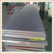
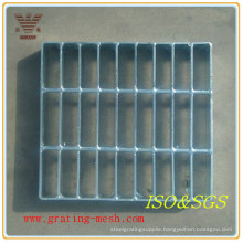
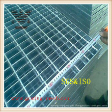
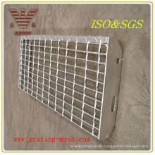
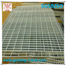
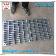
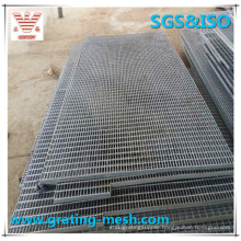
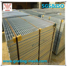
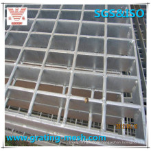
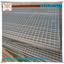
Framed SMT stencils
Framed SMT stencils or "glue-in" stencils are laser-cut solder paste stencils permanently mounted in a stencil frame using a mesh border to tightly stretch the stencil foil taut in the frame. Framed stencils are designed for high volume screen printing on printed circuit boards. Framed SMT stencils have smooth aperture walls and can be used for 16 Mil pitch and below and for Micro BGA's.
Framed SMT Stencil Features:
- Unique Process for smooth aperture walls
- Very clean laser-cut apertures
- Excellent print performance
- Excellent for high-volume stencil printing on printed circuit boards
- Unique process creates permanent non-removable non-fading fiducial
- All framed SMT stencils are double bonded to extreme wear
- 24-hour turnaround standard
Framed SMT PCB Stencils printer


Why choose us?
- Save money&time! Achieve peace of mind!
- A professional and trustworthy PCB prototype manufacturer.
- Fastest PCB Prototype.
- One stop solution for various PCB&SMT Stencil.
- Low cost for simple PCB.
- Affordable price for high-tech PCB.
- Minimum orders 1pcs.
- 24-hour online customer service.
- Professional PCB engineer for one-to-one service.
- Shipment on time.
- Guarantee good service and quality from PCB quotation to delivery.
Service features
- Custom PCB service.
- You get what you pay for!
- 7*24 hours Online service.
- Professional Technical support.
- Fast turnarounds.
- Fast delivery.
Certification(UL:E466618, TS16949, ISO9001.RoHS)
 |  |  |
PCB Shipment
JHY PCB offers flexible shipping methods for our customers, you may choose from one of the methods below.

Shipping Process
After production and testing, your PCB orders will be sent to our shipping department. As the quick turn PCB manufacturer, JHY PCB shipping department will ship your PCB quickly without any pending.
JHY PCB 's Packing Way
- Use one professional PCB vacuum bag, with desiccant inside. Vacuum compressed totally.
- Paste label and RoHs mark. Use second vacuum bag to protect boards again, vacuum compressed, make sure no exception.
- Microsection report and Tin testing board are put together with PCB in cartons.COC (Certificate of Conformity) will be sent to customer by email in PDF.
- Several layers of thick EPE(Expand aple poly ephylene) are filled fully in gaps between PCBs and cartons. Thickness of 1 layer EPE is 10mm.
- Neutral Packing is adopted if no special requirements. Strong and thick cartons(Thickness:10mm,7 layers). Different sizes of cartons are designed to meet demand of different PCB size. All package are within weight limit of cartons. For mass production order, no exceed 21kg per carton normally.
- All cartons sealed with strong adhesive tape should be sealed twice so as to make them more durable.
- Solid PP/PET strapping is used outside of cartons.
- Shipping mark, fragile mark and postcode label are all pasted clearly.
How to ship your PCB?
- Firstly, JHY PCB shipping department will print order address and invoice.
- Secondly, JHY PCB will set the shipment information on the Logistics company website.
- Thirdly, the Logistics company staff will collect the package from JHY PCB and ship it to you.
Shipment Term
With the purpose of better customer service and meeting the customer demand, JHY PCB provides following shipping methods.
JHY PCB is experienced in exporting. For PCB Prototype and small-medium volume PCB order, we have stable and long-term good relationship with forwarder, such as international express company DHL, FedEx, TNT, UPS. For mass production order, we have famous and reliable shipping company for support.
FAQ
Q1: What is your minimum order quantity?
A: Our MOQ is 1 PCS.
Q2: Do you accept PCB design with different boards on one panel?
A: Of course, we can do different boards on the same panel.
Q3. Are my Gerber Files safe?
A: We protect the intellectual property for customers in the whole process. All documents from customers are never shared with any third parties.
Q4: What is needed for quotation?
A: Quantity, PCB Gerber file, Technical requirements(material, board thickness, surface finish, copper thickness, solder mask color, silkscreen color,...)
Q5.How to quote shipping cost?
A: The shipping cost is determined by the shipment way(forwarder name, delivery days), destination, weight&dimension of packages. If you use your own forwarder, please inform us.

Product Categories : PCB Stencil